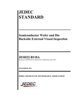
JEDEC JESD22-B118A
Semiconductor wafer and die backside external visual inspection is an examination of the external non-active surface area (hereafter called backside) of processed semiconductor wafers or die. This inspection method is for product semiconductor wafers and dice prior to assembly. This test method defines the requirements to execute a standardized external visual inspection and is a non-invasive and non-destructive examination that can be used for qualification, quality monitoring, and lot acceptance. Alternate methods of inspection or techniques that provide assurance to Clause 6 elements are acceptable (e.g., functional testing, automated inspection equipment, in-line manufacturing operations, etc.).
This test method is applicable to:
– Backside inspection of semiconductor wafers and die. Wafers and die sampled for external visual inspection must be representative of final product.
This test method does not apply to or require any inspection, measurement, or analysis other than the procedure described in clause 5.0. Recommended tools and equipment for this test method are presented in clause 4.0; use of substitute tools or equipment to perform this test method is acceptable provided correlated results are obtained.
Product Details
- Published:
- 11/01/2021
- Number of Pages:
- 20
- File Size:
- 1 file , 740 KB
- Note:
- This product is unavailable in Belarus, Russia, Ukraine


